Home » Cadence University Program » 2013 Research Projects Using Cadence Tools » Cadence Tool Use – Using Cadence Tools for RF Degraded Performance Model Development
Cadence Tool Use – Using Cadence Tools for RF Degraded Performance Model Development
Total Ionizing Dose (TID) causes parametric degradation in transistor DC parameters such as drain current (ID), small-signal transconductance (gm), which in turn causes degradation in transistor level RF parameters such as fT, fMAX and S-parameters. RF circuit performance depends on these parameters and hence would be affected by TID. The figure below shows the degradation in Id-Vg from TID experiments on a 24 µm wide (12 fingers each 2 µm wide) floating-body NMOSFET (length of 56 nm) fabricated in a 45 nm CMOS SOI technology.
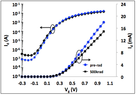
Id-Vg for NMOSFET before irradiation and after 500 krad(SiO2) irradiation at 25 ºC There is an increase in OFF state leakage and decrease in ON state current with TID at both temperatures.
There is an ON state degradation as well as increase in OFF state current. In the ON state, there is decrease in threshold voltage (VTH) and mobility (µn) of the device. The parameters of the SPICE-level transistor-model (BSIM) are useful in characterizing the operation of a device. For example a typical model file contains the model parameters for a transistor fabricated in the technology. The variable u0 and vth0 denotes the mobility and threshold voltage in a typical model file. These represent these parameters before irradiations. The TID degraded Id can be obtained by changing these to the values corresponding to a specific TID (obtained from the figure below).
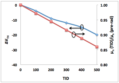
Change in VTH and mobility as a function of TID for 25 ºC. VTH decreases by 20 mV and mobility by 14% from pre-irradiation to 500 krad(SiO2).
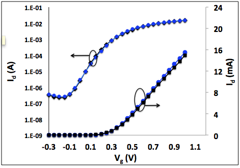
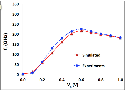
The figures below compare simulated and experimental Id-Vg, gm-Vg, fT, S21 of the NMOSFET at 500 krad (SiO2). There is < 5 % error between the simulated and experimental values.
The effects of these transistor level degradations at circuit level can be predicted by simulating RF circuits. The figure below shows a schematic diagram of a 22 GHz quadrature LC-VCO designed in CADENCE SPECTRE. The NMOSFET (24 µm wide, 12 fingers, 56 nm long, floating body) was used as unit cell for all the NMOSFETs in the circuit. Hence, the TID-aware compact model of NMOSFET can be used to simulate the performance degradation of the VCO.
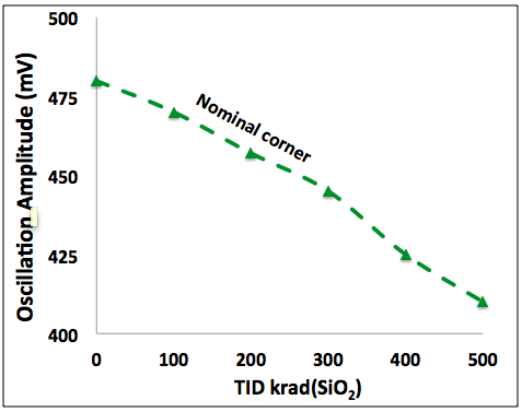
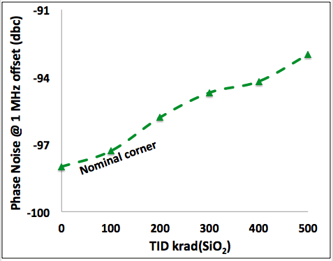
The figures below show the amplitude, frequency and phase noise degradation at 500 krad (SiO2). The VCO shows degradation of 240 MHz, 70 mV and 5 dBc in frequency, amplitude and phase noise at 500 krad(SiO2) compared to pre-irradiation.




Connect with RER
©2024 Vanderbilt University ·
Site Development: University Web Communications