Home » Cadence University Program » 2013 Research Projects Using Cadence Tools » Cadence Tool Use – Single-Event Transient Pulse-Width Measurement in Advanced CMOS Technologies
Cadence Tool Use – Single-Event Transient Pulse-Width Measurement in Advanced CMOS Technologies
Semiconductor based systems utilized in a space environment are subject to a number of extreme environment effects including:
- Temperature extremes
- Operation in a vacuum
- Radiation environments
A particular concern for the use of advanced CMOS technologies in space deals with the fact that ionizing particles incident on the semiconductor material cause information corruption and generate transient signals that compete with legitimate signals propagating through the circuit (clock trees, control paths, digital logic chains, etc) [1]. It is important to understand the potential distribution of transient pulse widths that could be produced as a result of the ionizing particle strike.
Traditional methods for characterizing these pulse widths includes fabricating a long chain of serially connected inverters, 100’s to >1000, and measuring the transient pulses at the output as a result of exposure to a heavy-ion accelerator beam. One issue that has been observed recently in SOI processes is the broadening of transient pulse widths in long serially connected inverter chains [2].
Using the Cadence tools, we designed and characterized a new test circuit design methodology to mitigate the pulse broadening effects and to allow us to characterize other sources of measurement skew. We’ve implemented this methodology in the design of two test chips, specifically for characterization of expected single-event transient pulse-widths. In the course of the design, we developed a basic digital logic library with schematics and symbols built in Virtuoso Schematic Editor and layouts developed in Virtuoso Layout Suite. We performed simulations of the basic cells using Spectre and we performed simulations of the full transient generation target and measurement circuit using UltraSim. The simulations increased our confidence that the design would function as intended before sending the design out for fabrication through MOSIS. The methodology and results from testing the fabricated circuits are shown below.
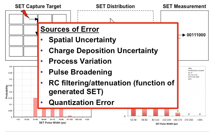
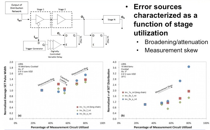
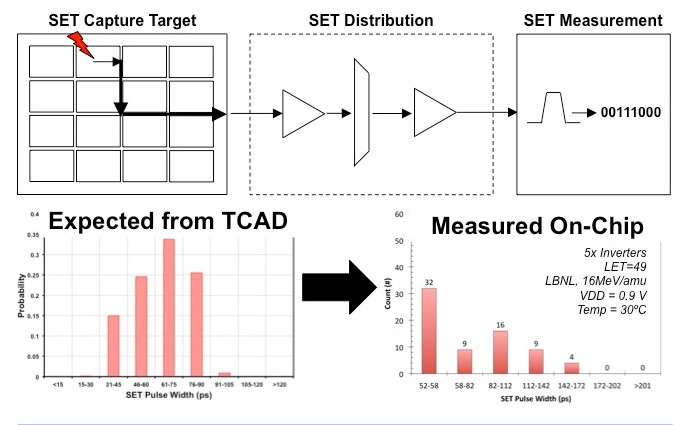 There are a number of sources of error in the on-chip measurement system. It can be seen that the expected gaussian distribution from striking a 3D TCAD device is not directly observed in measurement. We utilized some designed in capability to quantify these sources of error and we utilized simulation to further characterize them.
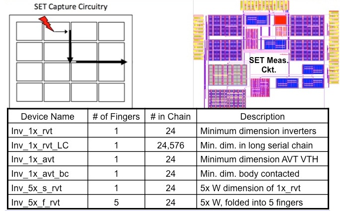
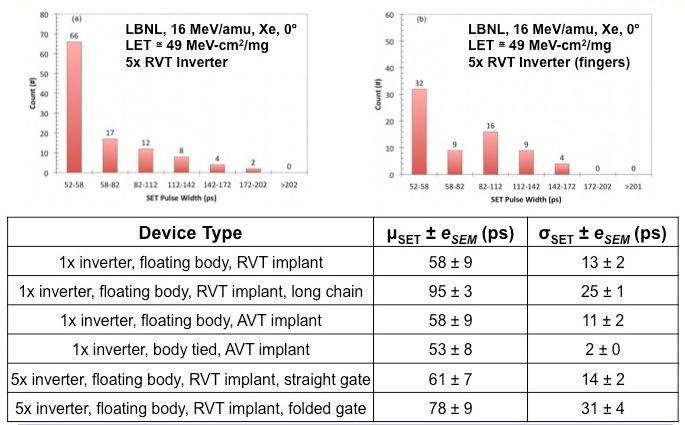
We developed a target design that utilized short chains of serially connected inverters, with the output of the short inverter chains being combined with an OR-gate tree. These short chains mitigated the pulse broadening effects that have been observed in long chains of serially connected logic. We did include a long chain on this chip, as denoted by Inv_1x_rvt_LC. All targets contain the same number of inverters, but the short chain targets only had 24 inverters per individual chain.
We did a custom placement and routing of cells to ensure that the parasitic impedance seen at the output of each short chains of logic would be identical across the target the design. This helped to remove an bias related to the chain that was struck within the target design. The result was a very symmetrical target design.
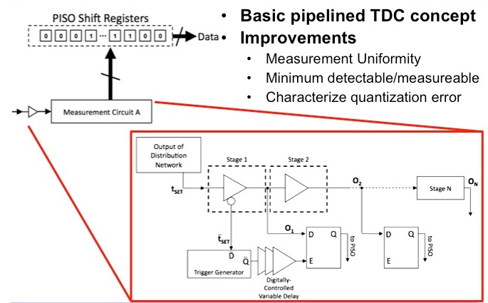
The pulse measurement circuit is a basic pipelined time-to-digital converter concept. We designed in the capability to characterize an skew introduced in the pipeline, a result of broadening of the transient, and the capability to understand the quantization error.
Using a combination of test data analysis, circuit layout inspection, and circuit simulation with Spectre, we were able to identify and quantify sources of measurement skew in the circuit.
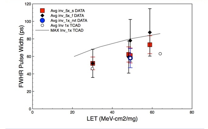
We checked our measured data by injecting voltage pulses from 3D TCAD simulations into the first inverter in a short chain. We performed simulations in Spectre, with layout parasitics included, and were able to achieve a qualitative agreement with data and even roughly reproduce the data quantitatively.
Using the design, we were able to compare pulse widths for multiple inverter types and compare them to expected TCAD based results. The use of simulation was critical in characterizing and understanding the sources of skew, allowing us to understand and interpret our measured data set.
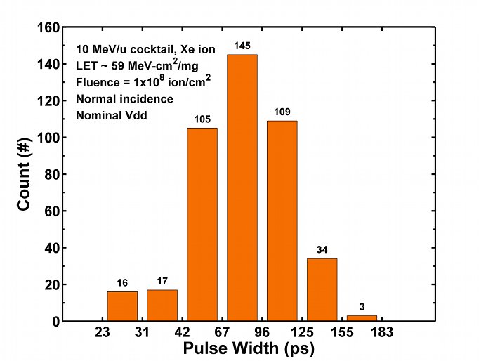
In a second pass design, in a more advanced technology, we were able to further overcome some of the parasitic impendances that resulted in the filtering of short SET pulses. We were able to measure a more gaussian looking distribution and compare to results from a similar second pass chip at the 45nm technology node.
[1] P. Dodd, M. Shaneyfelt, J. Felix, and J. Schwank, “Production and propagation of single-event transients in high-speed digital logic ICs,” vol. 51, no. 6, pp. 3278–3284, 2004.
[2] Ferlet-Cavrois, V.; Paillet, P.; McMorrow, D.; Fel, N.; Baggio, J.; Girard, S.; Duhamel, O.; Melinger, J. S.; Gaillardin, M.; Schwank, J.R.; Dodd, P.E.; Shaneyfelt, M.R.; Felix, J.A., “New Insights Into Single Event Transient Propagation in Chains of Inverters—Evidence for Propagation-Induced Pulse Broadening,” Nuclear Science, IEEE Transactions on , vol.54, no.6, pp.2338,2346, Dec. 2007
This work was published in IEEE TNS in 2012 and the updated 2nd pass work was presented at the 2013 IEEE NSREC. Both references are provided on the main 2013 Research Page





Connect with RER
©2024 Vanderbilt University ·
Site Development: University Web Communications